

DC Voltage Doubler Circuit using NE555 Timer IC
Hello friends! Welcome back to ElectroDuino. This blog is based on the DC Voltage Doubler Circuit using NE555 Timer IC. Here we will discuss Introduction to DC Voltage Doubler Circuit, Project Concept, Block Diagram, components required, circuit diagram, working principle.
Introduction
The Voltage Doubler is one type of electronic circuit, it gives output voltage which is equal to twice of the input voltage. This circuit is very useful when a higher voltage is needed out of a single lower voltage power supply. For example, many times, we need 10 volt power input in our projects, but if we have 5 volt power supply, in this condition we can use this circuit in our project to fulfill your requirements. This Voltage Doubler circuit input voltage stays between 3v to 12v and it generates output voltage approx 6v to 20v.
Project Concept
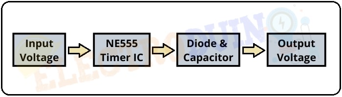
This is a very simple project. The key components of this project are the NE555 Timer IC, Diode, and Capacitor. We can divide the circuit into two parts, the first part consist of the NE555 time IC, which generates the square wave, and the second part consists of 2 diodes and 2 capacitors to double the output voltage. This circuit generates the output voltage by the charging and discharging of the capacitor through the diodes.
DC Voltage Doubler Circuit using NE555 Timer IC Block Diagram
Components Required
| Components Name | Quantity |
| NE555 timer IC | 1 |
| 1N4007 Diode | 2 |
| 470 µf Capacitor | 2 |
| 0.01µF Capacitor | 2 |
| 10k ohm Resistors | 1 |
| 33k ohm Resistors | 1 |
| 3V to 12v Power Supply | 1 |
| PCB board | 1 |
| Connecting Wire | As required in the circuit diagram |
Tools Required
| Tools Name | Quantity |
| Soldering Iron | 1 |
| Soldering wire | 1 |
| Soldering flux | 1 |
| Soldering stand | 1 |
| Multimeter | 1 |
| Desoldering pump | 1 |
| Wirecutter | 1 |
DC Voltage Doubler Circuit Diagram

Working Principle of DC Voltage Doubler Circuit using NE555 Timer IC
In this project, the NE555 timer IC configured in Astable multivibrator mode, in this mode this IC generates the square wave of approx 2KHz frequency. This output frequency is set by the resistor R1, R2, and capacitor C1.This output frequency set using the below formula:
F = 1.44 / (R1+2*R2) * C1
When the timer IC output (PIN 3) of 555 is low, this time the Diode D1 gets forward biased, and the capacitor C3 gets charged through this Diode (D1). Then this capacitor (C3) gets charged up to the same voltage of the input voltage (6v). When the timer IC output (PIN 3) of 555 becomes High, this time the Diode D1 gets reverse biased and blocks the discharging of the capacitor C3. But at the same time, D2 is forward biased and the capacitor C4 gets charged through this Diode (D2).
Now the output voltage of this circuit is equal to the capacitor C4 charges with the combined voltage of Capacitor C3 (6v) and the input voltage (6v), it means the circuit output is 6v of capacitor C3 and 6v of input supply voltage, so it charges up to 12v (twice the voltage of input source).


I don’t see the block diagram nor the circuit diagram. The project is useless without one or both of these.
sorry, the blog was not complete back then. Now it’s totally updated. Please do visit and check them out. Also, check the other blog post on this website. Thanks for visiting