
Time Delay Circuit using 555 Timer IC
Hello friends! Welcome back to ElectroDuino. This blog is based on How to Make Time Delay Circuit using 555 Timer IC. Here we will discuss the Introduction to the Time Delay Circuit using 555 Timer IC, Project Concept, Block Diagram, Components Required, Circuit Diagram, and Working Principle.
Introduction
All of us are facing a problem, sometimes we turn on our AC or DC Home appliances then forget to switch them off the appliances, which loss of electricity as well as can damage your appliances. A Time Delay Circuit is an electronic circuit that automatically turns on/off any load connected with its output after a fixed duration. The time delay circuit is very helpful when we need to power On/Off any AC Appliance / DC Appliance after a predefined duration. For example, Many times we keep our phone on charging and busy with other work due to overcharging the phone can be damaged. But using this circuit we can turn off the phone charger automatically and protects our phone from overcharging.
Block Diagram of Time Delay Circuit using 555 Timer IC

Components Required
| Components Name | Quantity |
| 555 Timer IC (IC1) | 1 |
| BC547 Transistor (Q1) |
1 |
| 1MΩ Potentiometer/Pot (VR1) | 1 |
| 10 KΩ Resistor (R2) | 1 |
| 150Ω Resistor (R3) |
1 |
| 220Ω Resistor (R4) | 1 |
| 470 µF, 16V Electrolytic Capacitor (C1) | 1 |
| 0.01µF Ceramic Capacitor (C2) |
1 |
| 10uf/16v Electrolytic Capacitor (C3) | 1 |
| Red LED (D1) | 1,1 |
| 1N4007 Diode (D1) | 1 |
| 5V Relay (K1) | 1 |
| 9V to 12V 1A Power Supply Adapter | 1 |
| PCB board | 1 |
| Connecting wires | As required in the circuit diagram |
Tools Required
| Tools Name | Quantity |
| Soldering Iron | 1 |
| Soldering wire | 1 |
| Soldering flux | 1 |
| Soldering stand | 1 |
| Multimeter | 1 |
| Desoldering pump | 1 |
| Wirecutter | 1 |
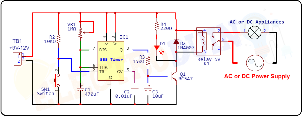
Circuit Diagram/ Schematics of Time Delay Circuit using 555 Timer IC
Looking for a reliable and high-performance Time Delay Circuit Board Design? Look no further than fscircuits, your trusted partner in professional PCB layout and design services.
Working Principle of Time Delay Circuit using 555 Timer IC
To better understand of working principle of the time Delay Circuit using 555 Timer IC here we have divided the circuit into two parts. One is Timer Circuit that is built around the 555 timer IC and the other one is the Switching Circuit that is built around the BC547 transistor.
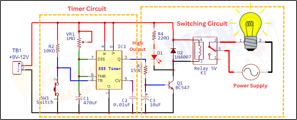
- Timer Circuit:
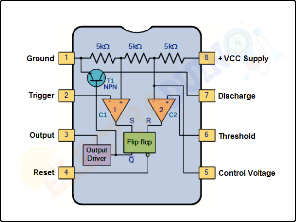
In this Time Delay circuit, the 555 Timer IC is configured in the Monostable mode. Before starting to understand the working principle of the time delay circuit we need to keep the following 3 points in mind.
- Whenever the Trigger Pin (Pin-2) of the 555 timer IC senses any voltage less than 1/3rds of the supply voltage, then it turns ON the output (Output Pin gives High output).
- When the Threshold Pin (Pin-6) of the 555 timer IC senses any voltage more than 2/3rds of the supply voltage, then it turns OFF the output (Output Pin gives LOW Output).
- When the output of the 555 timer IC is in the OFF state, the Discharge Pin (Pin-7) of the 555 timer IC acts as ground/negative rail i.e, it is internally connected to 0V.
After Connecting all the components according to the circuit diagram, now turn on the power supply. Initially, the output of the 555 time IC will be in the stable state i.e. Output at PIN 3 is LOW (0V). Whenever the output is in an OFF state, the discharge pin (Pin 7) of the timer IC will be internally connected to 0V. This time the capacitor (C1) completely discharges and won’t be able to charge via the series resistor/potentiometer (VR1) that connects it to the positive input voltage.
When we press the momentary push button switch, then the delay timer is activated, and the following sequence happens in the circuit:
- When we press the push button switch (S1) the trigger pin is pulled low,i.e. 0V (Grounded) is applied at the trigger pin (Pin-2) of the 555 Timer IC.
- Because this applied voltage (Ground/0V) at trigger pin (Pin-2) is less than 1/3rd of the supply voltage (Vcc), the Lower comparator inside the timer IC becomes HIGH, and the Flip flop gets Set. As a result, the output turns ON and we get HIGH OUTPUT at the output pin (Pin 3).
- Simultaneously, Transistor T1 inside the timer IC becomes OFF, and Timing Capacitor (C1) gets disconnected from the Ground and starts charging through the Resistor/Potentiometer (VR1) that connects it to the positive rail, Since the threshold input pin (Pin-6) is connected to the positive terminal of the capacitor, it actively monitors the voltage across it.
This state is called the quasi-stable state and remains for some time (T). This time period for which the capacitor charges from 0V to 2/3rds of supply voltage is the delay time
Now when the capacitor charges reach to the voltage slightly greater than 2/3 of the supply voltage, then the voltage at the Threshold pin (Pin-6) becomes greater than the voltage at the inverting end (2/3Vcc) of the Upper comparator of the Timer IC.
- At this time the Upper comparator inside the timer ic becomes HIGH and the Flip flop gets Resets. As a result, the output turns OFF and we get LOW OUTPUT at the output pin (Pin 3).
- simultaneously, Transistor T1 inside the timer IC becomes ON, as a result, the discharge pin (Pin-7) is internally re-connected to the ground (0V) and the capacitor (C ) starts discharging through the Discharge PIN 7.
Calculating the Delay Period of the Time Delay Circuit:
The time period of the timer circuit can be determined by the RC (Resistor, Capacitor) network. The time period is equal to the time taken by the capacitor to charge from 0V to 2/3rd of the supply voltage. This duration can be calculated with the formulae given below:
T= 1.1 * R * C
where,
T = Time Period in seconds
R = values of timing Resistor is in OHM (Ω)
C= values of timing Capacitor is in Farads (F).
- Switching Circuit:
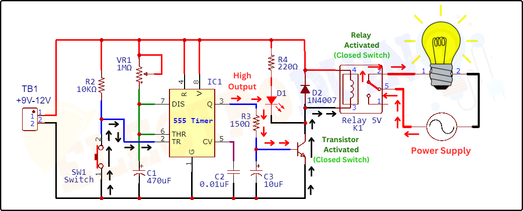
When Timer IC Output is HIGH:
When the Output pin of the 555 timer IC is High then this High output voltage appears at the base terminals of the BC547 Transistor (Q1) through the resistor (R). Here, the Transistor (Q1) works as a switch. So the high output voltage activates the Transistor and it works as a closed switch. As a result, the relay connects to the ground through the Transistor, which activates the relay and it works as a closed switch which turns ON the home appliance. The relay will be activated until the 555 timer IC output goes LOW.
When Timer IC Output is LOW:
When the Output pin of the 555 timer IC is Low then this Low output voltage appears at the base terminals of the BC547 Transistor (Q1) through the resistor (R). Now this Low output voltage deactivates the Transistor, then it works as an Open switch. As a result, the relay disconnected to the ground, which deactivates the relay and it works as an Open switch which turns OFF the home appliance. The relay will be deactivated until the 555 timer IC output goes High.