
RF Transmitter and Receiver Circuit using RF Module
Hello friends! Welcome back to ElectroDuino. This blog is base on RF Transmitter and Receiver using RF Module. Here we will discuss Introduction to RF Transmitter and Receiver, Project Concept, Block Diagram, components required, circuit diagram, working principle.
Introduction
The RF transmitter and receiver is an easy way to communicate (one way) two devices by radio frequency. The corresponding range varies between 30 kHz & 300 GHz, in the RF communication system, The digital data is represented as variations in the amplitude of carrier wave. This modulation is known as Amplitude shifting key (ASK). These signals transmitted through radio frequency (RF) can travel long distances. So, it can be used to communicate in long-range applications. RF communication uses a specific frequency range to communicate two devices. The signals on one frequency band in RF will not interfere by other frequency RF signals. The radio frequency signals can be transmitted when any obstacles between the transmitter and receiver.
Project Concept
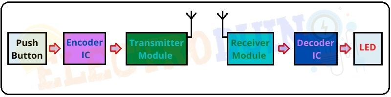
In this project, we will control 4 LED using 4 push button switch through RF wireless communication. The pushbuttons are connected to the encoder IC. This IC takes 4-bit data from these push button and convert into serial data, then send this data using RF transmitter module. Another side, the RF receiver module receives this serial data and provides it to the Decoder IC. Then the Decoder IC decodes this data and controls the LEDs.
Block Diagram of RF Transmitter and Receiver Circuit
Components Required
| Components Name | Quantity |
| 433Mhz RF Transmitter and Receiver Module | 1 |
| HT12D Decoder IC | 1 |
| HT12E Encoder IC | 1 |
| 7805 Voltage Regulator |
1 |
| 1M ohm Resistor | 1 |
| 33K ohm Resistor | 1 |
| 220-ohm Resistor | 1 |
| 0.1 uF Ceramic Capacitor |
1 |
| Push Button | 4 |
| LED (Red, Green, Blue, Yellow, and White) | Each 1`(total 5) |
| Bread Board or Dot PCB Board | 2 |
| 9v Battery with Battery Cap | 2 |
| Connecting wire | As required in the circuit diagrams |
Tools Required
| Tools Name | Quantity |
| Soldering Iron | 1 |
| Soldering wire | 1 |
| Soldering flux | 1 |
| Soldering stand | 1 |
| Multimeter | 1 |
| Desoldering pump | 1 |
| Wirecutter | 1 |
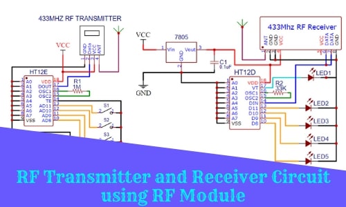
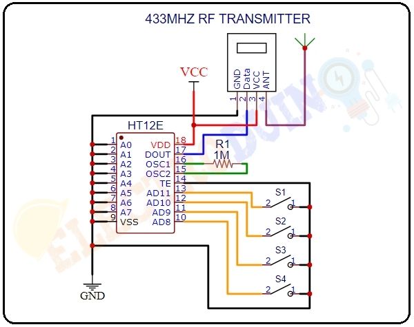
Circuit Diagram of RF Transmitter
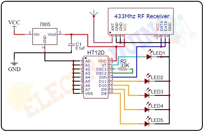
Circuit Diagram of RF Receiver
Circuit Description
Transmitter Circuit
The HT12E encoder IC VSS pin is connected to the power supply Ground (-) and the VDD is connected to the power supply VCC (+). IC A0 – A7 pins (pin 1 – 8) are connected to the Ground(-) to set the address at 0b00000000. The Switch 1 (S1), Switch 2 (S2), Switch 3 (S3), and Switch 4 (S4) are respectively connected to the AD11 (13), AD10 (12), AD9 (11), and AD8 (10). The 1M ohm resistor is connected between the pin 15 and 16, which provides the external resistance for the operation of the internal oscillator of the HT12E IC. The RF Transmitter module GND pin is connected to the power supply Ground (-) and the VCC is connected to the power supply VCC (+). The Data pin is connected to the DOUT (pin 17) of the IC.
Receiver Circuit
The HT12D decoder IC VSS pin is connected to the power supply Ground (-) and the VDD is connected to the power supply Vout (+) of the 7805 5v voltage regulator. IC A0 – A7 pins (pin 1 – 8) are connected to the Ground(-) to set the address at 0b00000000. The LED2, LED3, LED4, and LED5 are respectively connected to the D11 (13), D10 (12), AD9 (11), and D8 (10). The 33K ohm resistor is connected between pin 15 and 16, which provides the external resistance for the operation of the internal oscillator of the HT12D IC. The RF Receiver module GND pins are connected to the power supply Ground (-) and the VCC is connected to the power supply VCC (+). The Data pin is connected to the DIN (pin 14) of the IC.
How RF Transmitter and Receiver Circuit Works
The HT12E encoder IC’s 4 data pins are connected to the 4 push buttons. The push buttons provide 4-bit data to the HT12E encoder IC. Then the IC converts these 4-bit data into serial data and this serial data will be available at the DOUT pin (pin17) of the IC. This output serial data is given to the RF Transmitter module. Then the RF transmitter module transmits this serial data using radio signals.
At the receiver side, the RF receiver module receives this serial data coming from the transmitter. Then this serial data is given to the DIN pin (14) of the HT12D Decoder IC. Now the decoder IC will convert the received serial data into 4 bit parallel data. The 4 data pins of the decoder IC are connected to 4 LEDs, which is control according to the transmitted data from the transmitter.
When we will provide Power supply to both circuits and we should notice that all LEDs will start glowing. Because the push-button pins (IC pin D8-D11) are pulled up internally by the Encoder IC. If we will press one push-button the data pin is connected to the ground in the transmitter circuit, then the respective LED will be turned off in the receiver circuit.
For example, if we will press Switch 1 (S1) which connected to the AD11 (pin13) of the Encoder IC, then the LED 2 will turn off which is connected to the D11 (pin13) of the Decoder IC.