
PN Junction Diode – Formation, Symbol, Biasing, V-I Characteristics, Application
Hello friends! Welcome back to ElectroDuino. This blog is based on PN Junction Diode. Here we will discuss What is PN Junction and PN Junction Diode, Formation, Symbol, Biasing, V-I Characteristics, and Applications.
What is PN Junction?
If one side of a semiconductor material doped with acceptor impurities while the other side doped with donor impurities, then there the P-type region is created on one side of the semiconductor material and the N-type region on the other side. The interface or boundary between these two regions (N-type and P-type) is called a PN Junction.

How is a PN Junction Formed?
From the definition of PN junction, we can easily understand how the PN junction is created in an intrinsic or pure semiconductor material. When the one side of an intrinsic or pure semiconductor material (Like, Silicon (Si) and Germanium (Ge)) doped with acceptor impurities atom (Trivalent impurities atoms, like Boron (B), Gallium (G), Indium(In), Aluminium(Al)) to build it as a P-type semiconductor and the other side doped with donor impurities (Pentavalent impurity atoms, like Phosphorus (P), Arsenic (As), Antimony (Sb),) to build it as N-type semiconductor. Where these two regions (P-type and N-type) are meet together there PN junction is formed. The P-type region of the semiconductor has an excess of holes and the N-type region has an excess of electrons.
Diffusion and Drift are important processes that take place during the formation of a p-n Junction.
In the P-N junction Semiconductor material, the concentration of electrons in N-type region is more than the holes and the concentration of holes in P-type region is more than the electrons. These electrons repel each other due to high concentration in the N-type region. When a p-n junction is being formed, Due to repulsion, some electrons diffuse from the n-type region to the p-type region. They are recombined with the holes in the P-type region because the electrons are attracted by the holes. Then the region of P-type which is close to the P-N junction is takes on the negative charge and the other side, the region of N-type which is close to the P-N junction is takes on the positive charge because the electrons are departed from the N-type region. So, across the junction there is an inclination for the free electrons to diffuse into the P-type region and holes to the N-type region, and this process is known as diffusion.
Due to the diffusion of electrons and holes, an electric field region develop between the N-type and P-type region that is called the depletion region.
This electric field is responsible for the movement of electrons from the p-type region to the n–type region and holes from the n-type region to the p-type region. This movement of charged carriers (electrons and holes) due to the electric field is called drift.
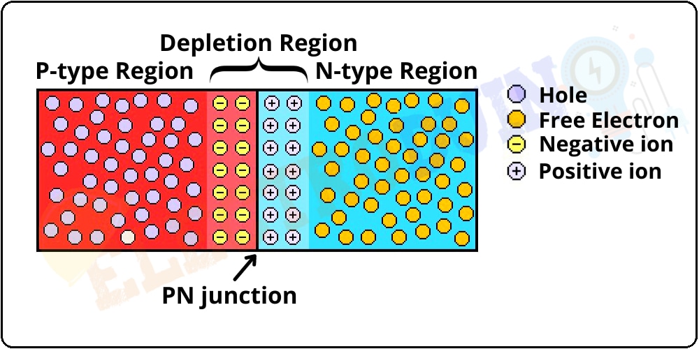
There is a voltage or potential difference across the junction due to the Positive ion in the N-type region and the Negative ions in the P-type region. This voltage or potential difference is called Built-in-potential or Barrier Potential. If an electron wants to move from the n-type region to the p-type region, it has to overcome this Barrier Potential. The Potential difference of a Silicon Diode is 0.7v and 0.3v for a Germanium Diode.
What Is a PN Junction Diode?
When the P-N junction semiconductor is used in circuits, this is known as the P-N junction Diode.
Definition of PN Junction Diode: A p-n junction diode is a two-terminal basic semiconductor device that controls the flow of electric current in a circuit. It allows the flow of electric current in only one direction and blocks the electric current in reverse (opposite) direction.
PN Junction Diode Symbol and Polarity
PN Junction Diode has two leads or terminals, these are connected to the P-type and N-type regions. The lead or terminal connected to the p-type region is called the anode or Positive terminal and the lead connected to the n-type region is the cathode or Negative terminal.
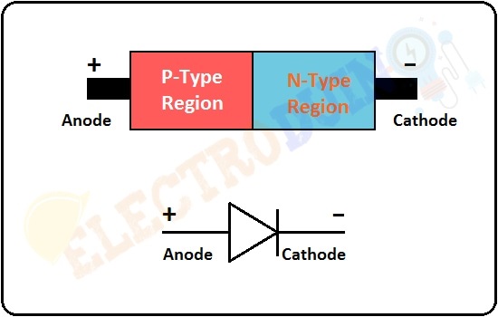
The symbol of a diode is like an arrowhead which front point has a bar. The arrowhead direction shows the direction of the current flow. We can easily identify the polarity by seeing the “bar” on the symbol, this side is the cathode or negative terminal. For the actual diode, a white line around the circumference of the diode, the side is the cathode or negative terminal.
Biasing of PN Junction Semiconductor Diode
The process of applying the external voltage to a p-n junction diode is known as bias. Based on the applied external voltage, there are three types of “biasing” possible for the P-N Junction Diode, these are:
- Zero bias: No external voltage applied to the p-n junction diode.
- Forward bias: The positive terminal of the external voltage potential is connected to the p-type (Anode terminal of Diode) and the negative terminal is connected to the n-type (Cathode terminal of Diode).
- Reverse bias: The negative terminal of the external voltage potential is connected to the p-type (Anode terminal of Diode) and the positive terminal is connected to the n-type (Cathode terminal of Diode).
Zero bias
In this case, when no external voltage or potential energy is applied to the P-N junction diode, then it is in equilibrium condition. This is also called a zero bias or unbiased p-n junction. The zero bias is the normal condition of a P-N junction diode. So, you have already seen what is happening inside the PN junction semiconductor in the “How is a PN Junction Formed” part.
Forward Bias
When the p-type region (Anode terminal of Diode) is connected to the positive terminal of the external voltage source (Like battery) and the n-type region (Cathode terminal of Diode) to the negative terminal, then the P-N junction diode is said to be connected in Forward Bias condition.

In this biasing, If this external voltage is greater than the value of the potential barrier (0.7 volts for silicon and 0.3 volts for germanium), then the negative terminal provides free electrons (negative charge carriers) in the n-type region. So the concentration of free electrons increases in this region, due to repulsion electrons get enough energy to pass through the depletion layer and combine with the holes. On the other side, the positive terminal provides holes (Positive charge carriers) in the P-type region. So the concentration of holes increases in this region, due to repulsion holes get enough energy to pass through the depletion layer. As result, the reduction in the number of positive and negative ions and neutralize the depletion region, and the width of the depletion region decreases.
While free electrons are combined with holes, then they become valence electrons. These valence electrons continuously travel in the p-type region, these electrons passing from one hole to the next until it reaches the end of the diode (at anode terminal). When a free electron leaves the left end of the diode (positive terminal), a new hole appears and the process starts again. In this way, the free electrons are attracted towards the positive terminal of the external voltage source and the holes are attracted towards the negative terminal of the external voltage source. For this reason, at the same time, billions of electrons are traveling from the negative terminal (cathode) to the positive terminal (anode), and continuously current flows across the diode.
Reverse Bias
When the p-type region (Anode terminal of Diode) is connected to the negative terminal of the external voltage source (Like battery) and the n-type region (Cathode terminal of Diode) to the positive terminal, then the P-N junction diode is said to be connected in Reverse Bias condition.

In this biasing, when the positive voltage applied to the N-type region, then the electrons in this region attract by the positive electrode (positive terminal of the external voltage source) and electrons flow away from the junction to the positive electrode and leaving behind the positive ions. On the other hand, when the negative voltage applied to the P-type region, then the holes in this region attract by the negative electrode (negative terminal of the external voltage source) and holes flow away from the junction to the negative electrode and leaving behind the negative ions. As result, the depletion layer grows wider. The width of the depletion region is directly proportional to the reverse voltage applied to the p-n junction diode. It means when the reverse voltage is increased then the width of the depletion region is also increases. The width of the depletion region stops growing when its potential difference is equal to the applied reverse voltage. As resulting, electrons and holes are cannot cross the junction for diffuse to the opposite region. So, due to the lack of movement of electrons and holes, there no current flows through the P-N junction diode.
V-I Characteristics of PN Junction Diode
The V-I characteristics of the PN junction diode is a voltage Vs current graph, that explains the relationship between voltage and current in a Diode.

When the PN junction diode is in forward bias, at zero voltage, zero current will flow through the diode. If the applied voltage is less than the barrier potential, a small current flows through the diode. But, when the applied voltage exceeds the barrier potential, the current starts flowing through the diode and increases rapidly. This applied voltage value that will start the current flow through the diode is known as forward voltage or VF of a diode. It is also called knee voltage.
When the PN junction diode is in reverse bias, at the zero reverse voltage no current flows through it. If the reverse voltage increases a very small current starts flowing through the diode, that known as Reverse Leakage Current. This reverse current is so small, its range of 0.000000001A or 1nA, that’s has no notable effects in a circuit, and it is considered almost zero.
After a certain point when you further increase the reverse voltage, the diode starts conducting heavily in the reverse direction and the current starts flowing rapidly through the diode. This process called Avalanche Breakdown and this voltage is known as Reverse breakdown voltage.
Why silicon is more preferred over germanium to design Diodes
There are two important points we can easily understand why silicon is more preferred over germanium to make Diodes. Also, we can see the difference between the Diodes made of silicon and the Diodes made of germanium.
| Diodes made of silicon | Diodes made of germanium | |
| Forward bias voltage | Approximately 0.7 volts | Approximately 0.3 volts |
| Working temperature | Works at high temperature | Working temperature is less than silicon. At high temperatures, the Germanium crystal structure is destroyed. |
Application
P-n junction diode is mainly used in:
- Clipping circuits for waveshaping
- Clamping circuits for DC restoration
- Voltage multipliers
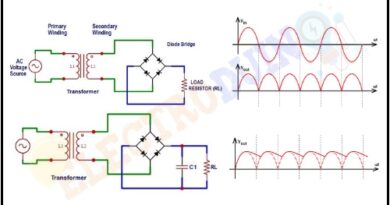
- Rectifier circuit
- Used in demodulation circuits
- Forward bias condition is used in all Light Emitting Diodes (LED) lighting applications.