

Full Wave Bridge Rectifier – Circuit Diagram and Working Principle
Hello friends! Welcome back to ElectroDuino. This blog is based on Full Wave Bridge Rectifier. In the previous tutorials, we have already discussed Half Wave Rectifier and Center -tapped Full Wave Rectifier. Here we will discuss what is Full Wave Bridge Rectifier, Working Principle, Circuit Diagram, Waveforms, Formula, Advantages, and Disadvantage.
Full Wave Bridge Rectifier
A bridge rectifier is a type of full-wave rectifier that uses four individual rectifying diodes connected together in a closed-loop bridge configuration to efficiently convert the Alternating Current (AC) into Direct Current (DC). It can rectify both half-cycles of an AC input sine wave.
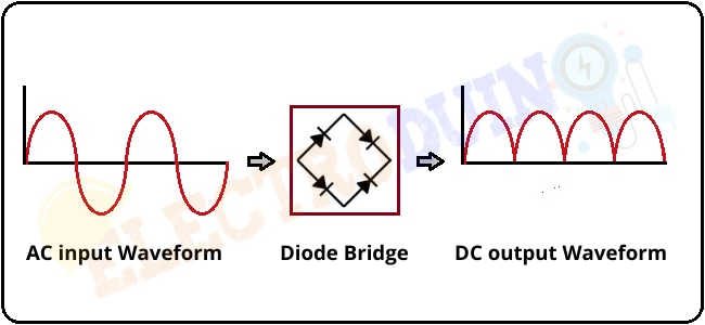
This Rectifier circuit produces the same output waveform as the full-wave rectifier circuit. The main advantage of the Bridge Rectifier is that the expensive center-tapped transformer is not used in this design, a normal transformer is used in place of a center-tapped transformer. So, the size of the circuit will be reduced, as well as its cost also reduced. For this reason, full-wave bridge rectifiers have practical applications much more than center-tapped full-wave rectifiers.
|
Also, See |
Construction of Full Wave Bridge Rectifier
The full-wave bridge rectifier circuit is constructed with four diodes (D1, D2, D3, D4), a Normal transformer, and a load resistor (RL). The four diodes are connected together in a closed-loop bridge configuration. The following figure shows the circuit diagram of the Bridge rectifier:
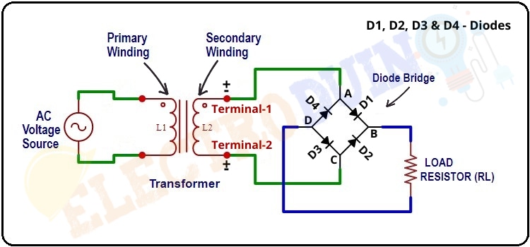
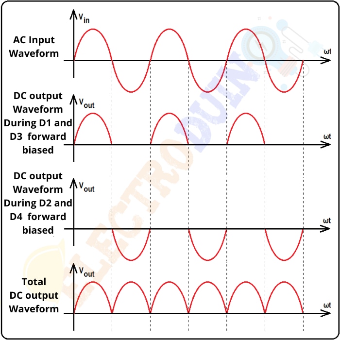
These diodes are arranged in series pairs that only two diodes conduct current during each half cycle. For example, during the positive half cycle of the AC input, diodes D1 and D3 conduct in series which allows electric current to pass, but this time diodes D2 and D4 are reverse biased which block electric current. During the negative half cycle of the AC input, diodes D2 and D4 conduct in series which allows electric current to pass, but this time diodes D1 and D3 are reverse biased which block electric current. The transformer is used to convert the high-level AC voltage into low-level AC voltage because the high-level AC voltage input can destroy diodes. The secondary winding of the transformer is connected to two diametrically opposite points of the bridge at points A & C and the load resistance (RL) is connected to the other two diametrically opposite points of the bridge at points B & D. We get output DC voltage across the Load Resistor (RL).
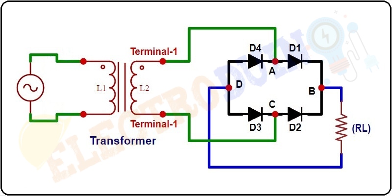
If we simplify this rectifier circuit to better understanding, then the circuit diagram looks like the following figure:
Working Principle of Bridge Rectifier (Theory)
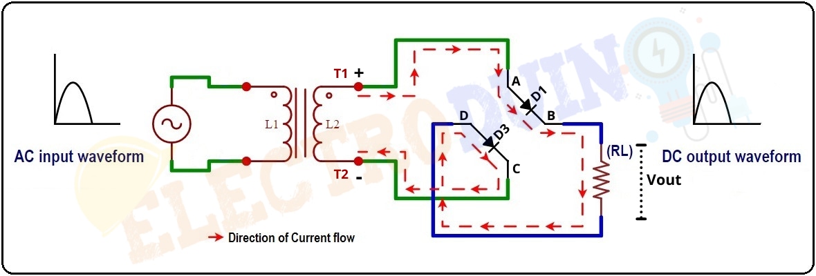
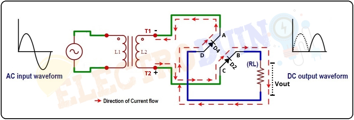
During the positive half-cycle of the AC input voltage, terminal-1 (T1) of the transformer secondary winding is positive (+) with respect to Terminal-2 (Ground). In this condition, diodes D1 and D3 are forward-biased. So, the current flows through diode D1 (AB arm), enters into the load resistance (RL), then it flows through diode D3 (arm DC), and returns to terminal-2 (ground). But, diodes D4 and D2 are reverse biased blocking the current to flow through diodes D2 (AD and BC arm). So, only the positive voltage appears across the load resistor.
The following figure shows the output of the Full-Wave Bridge Rectifier during the Positive Half Cycle. The diodes D4 and D2 are reverse biased, therefore we will omit the diodes D4 and D2 from the rectifier circuit, which helps us to better understand the direction of current flow in the circuit.
During the negative half-cycle of the AC input voltage, terminal-2 of the transformer secondary winding is positive (+) with respect to terminal-1 (Ground). In this condition, diodes D2 and D4 are forward-biased. So, the current flows through diode D2 (CB arm), enters into the load resistance (RL), then it flows through diode D4 (arm DA) and returns to terminal-1 (ground). But, diodes D1 and D3 are reverse biased that block the current to flow through diodes D1 and D3 (AB and DC arm). In this case, again the positive voltage appears across the load resistor as before.
The following figure shows the output of the Full-Wave Bridge Rectifier during the Negative Half Cycle. The diodes D1 and D3 are reverse biased, therefore we will omit the diodes D1 and D3 from the rectifier circuit, which helps us to better understand the direction of current flow in the circuit.
As a result, we get the DC output voltage across the load resistor. This output voltage has the same polarity and this output current is in the same direction. The DC output voltage across the load resistor is a series of positive half cycles or positive sinusoidal pulses. In this way, this rectifier converts the AC input voltage into a DC output voltage.
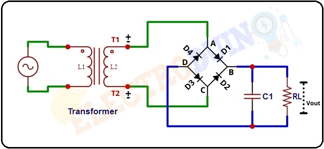
Full Wave Bridge Rectifier with Capacitor Filter
The output of a full-wave bridge rectifier is a pulsating DC voltage with lots of ripples that increases to a maximum and then decreases to zero. Generally, this kind of DC voltage has no practical applications. So, we need to convert pulsating DC voltage into a smooth DC voltage that can be done by a filter. Here we will use a capacitor as a filter that is parallelly connected to the load resistor (RL).
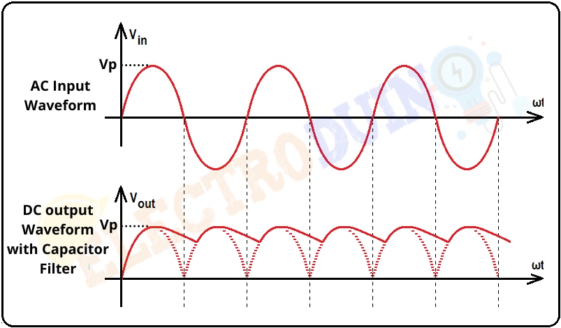
Initially, the capacitor is uncharged. During the first positive half-cycle, the diode D1 and D3 are forward biased, at the same time the capacitor starts charging. The capacitor charging continues until the input reaches its peak value (Vp). At this point, the input voltage is equal to the capacitor voltage. After the input voltage reaches its peak value then it begins to decrease. When the input voltage is less than Vp, at the same time capacitor starts discharging through the load resistor and supplies the load current, until the next peak arrives.
During the negative half-cycle, the next peak arrives, this time diode D2 and D4 are forward-biased. So, again the capacitor starts charging until the input reaches its peak value (Vp). When the input voltage is less than Vp, again capacitor starts discharging through the load resistor and supplies the load current, until the next peak arrives.
This process happens again and again. As a result, we get a Smooth DC output voltage across the load resistor (RL).
Advantages
- Use of transformer: A bridge rectifier can be made with or without a transformer. If a transformer is used to make this circuit, we can use any normal step-down/step-up transformer to made it.
- High rectifier efficiency: The rectification efficiency of a full-wave bridge rectifier is double that of a half-wave rectifier. So, it can convert the AC voltage to DC voltage more efficiently of the bridge as compared to the half-wave rectifier.
- Low ripples: The output of a bridge rectifier has less ripples as compared to the half-wave rectifier. However, the ripple factor of both the bridge rectifier and the center-tapped full wave rectifier is the same.
- Low power loss: It is allowed both positive and negative half cycles of the input AC voltage. So the output power is almost equal to the input power.
- High TUF: Transformer utilization factor (TUF) is higher as compared with a center-tapped rectifier.
Disadvantages
- It needs four diodes for construction.
- The construction and design of the bridge rectifier circuit are more complex than the half-wave rectifier and center-tapped full-wave rectifier.
- This rectifier needs four diodes to construct, therefore its cost will be high.


