
BD139 Transistor – Pinout, Specifications, Datasheet
Hello friends! Welcome back to ElectroDuino. Hope you all are doing well. This blog is based on the BD139 Transistor – Pin Diagram, Specifications & Working Principle. Here we will discuss the Introduction to the BD139 transistor, Pin diagram, How it Works, Specification, Features, Equivalent, Applications, and Download Datasheet.
Introduction:

A semiconductor device used to amplify electrical signals and power is called a transistor. BD139 is a BJT (Bipolar Junction Transistor) NPN Transistor, basically used in many electronic circuits as switches or amplifiers like in motors, relays, high power LEDs, etc. it is in the plastic package of TO-126, TO-225 and SOT-32. This transistor has a gain value of ranges from 40 to 160 which determines the amplification capacity for the transistor.
Its saturation voltage is 0.5 V and collector terminals dissipation current is 12.5 W with high collector-emitter and collector-base voltage. BD139 has a current limit of 1.5 A.
Pin Configuration/ Pin Diagram/ Pinout of BD139 Transistor:
Like every other transistor even BD139 has three terminals mentioned below;

| Pin No. | Pin Name | Symbol | Functionality |
| 1 | Emitter | E | The emitter terminal is normally connected to the GND terminal of the power supply and this terminal drains out the current. |
| 2 | Collector | C | The collector terminal is normally connected to the load, the current flows in through this terminal. |
| 3 | Base | B | The base terminal is used to control the transistor biasing; it means this terminal is used to switch ON/OFF the transistor. |
Note: Download the BD139 datasheet given at the end of this page to get Complete Technical Details.
Working principle of BD139 Transistor
As mentioned BD139 is an NPN transistor, so, in it the p-doped layer is embedded between two n-dopped layers. The collector and emitter are left open when the base pin is held at the ground and are closed when a signal is provided to the base pin. Since BD139 is an NPN transistor so the majority of charge carriers are electrons.
When the sufficient current is applied to the base terminal, then it will work in forward biased condition and it turns on. In this condition, the maximum current drawn by the emitter and collector is 1.5A. If the maximum current of 1.5A is supplied throughout this transistor then it will be in Saturation Region. And the magnitude of this supplied current must be more in than the collector current. The maximum voltage that can be provided across emitter and collector terminals is 80 V.
When no current is applied at the base terminal of this transistor, it turns off and this situation is termed as cut-off region.
How to use BD139 Transistor?
The BD139 transistors have numerous use in the applications of switches and amplifiers i.e., the two main uses of any transistor existing in the electronics arena.
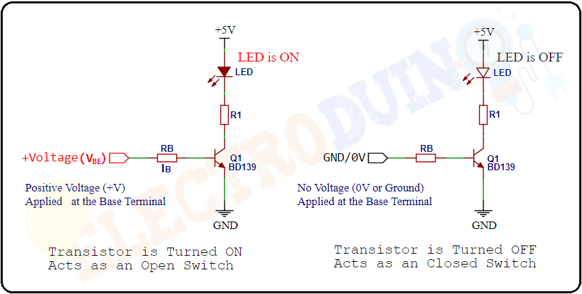
Transistor Work as a Switch
The BD139 transistor can be used as a switch to control lamps, relays, or even motors. Here we are using a simple circuit to easily understand how it works as a switch. The emitter terminal is connected to the ground of the power supply, the collector terminal is connected to the positive power supply through a load, here we have used a LED as load. The input voltage is applied to the base terminal to control the transistor biasing.
When the sufficient positive voltage/current is applied to the base terminal, then it will work in forward biased condition and it turns on and acts as a closed switch. In this condition is said to be the transistor is in its Saturation region. This time transistor allows to flow of the current from the Collector to Emitter, so the current also flows from the source (+5v) to the ground through the load (LED). As a result, LED starts glowing.
When the no voltage/current is applied to the base terminal, then the transistor will work in reverse biased condition and it turns on and acts as an open switch. In this condition is said to be the transistor is in its cut-off region. This time transistor does not allow to flow of the current from the Collector to Emitter, so No the current also flows from the source (+5v) to the ground through the load (LED). As a result, LED is turned OFF.
Transistor Work as an Amplifier
The transistor is used as an amplifier to raise the strength of a weak input signal. The input signal of an amplifier is a voltage or a current, and the output is an amplified version of the input signal. So the transistor accepted a weak signal as input through the emitter-base junction and produces the amplified signal as output through the collector-base junction. The DC input signal is applied at the emitter-base junction, which makes it remain in forward biased condition.

Specifications and Features of Bd139 Transistor:
The features and specifications of BD139 are listed below which makes it very versatile for wide range of uses;
- Transistor Type – NPN
- Package – TO-126 and TO-225
- The case used – Plastic case
- Maximum Collector-Emitter voltage VCB: 80 V
- Maximum Collector-Base voltage VBE: 5 V
- Emitter Base Breakdown Voltage (VBE): 5V
- Base Current (Ib): 0.5A
- Maximum Collector Current (IC): 1.5 A
- Collector Dissipation factor: 12.5 W
- Maximum Transition Frequency (fT): 190 MHz
- Range of junction temperature for operating and storage: 55 to 150 oC
Equivalent Transistors of BD139 Transistor:
The transistors equivalent for the BD139 transistor are BD169, BD179, BD230 or MJE244.
Advantages:
- It can be of great use in Arduino circuits.
- It can handle current up to 1.5 A
- It is having comparatively low cost.
- It has quite a long life.
- Its plastic package makes it versatile for many uses.
Applications:
- They are used in load driver circuits.
- Like all other transistors, even BD139 transistors are used for switching purposes.
- They are also used for amplification purposes.
- Audio amplification is one of its main domains.
- They also have applications in RF amplifiers.
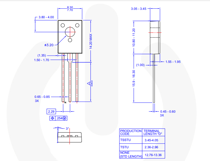
2D-Model and Dimensions (TO-225)
Download Datasheet