
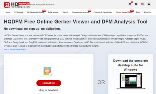
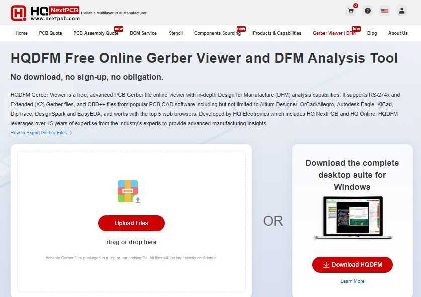
HQDFM Free Online Gerber Viewer and DFM Analysis Tool
In the realm of electronics and technology, Printed Circuit Boards (PCBs) serve as the backbone, enabling the seamless integration of electronic components. As the demand for more sophisticated and compact electronic devices continues to grow, the importance of precise PCB design and manufacturing cannot be overstated.
NextPCB.com, a leading player in the PCB industry, introduces the HQDFM Free Online Gerber Viewer and DFM Analysis Tool, a game-changing platform designed to redefine the landscape of PCB ( printed circuit board) design. With features like “Check PCB manufacturing data the smart way, Identify Design for Manufacture issues in seconds, and Fast-track ordering with HQ NextPCB,” HQDFM is set to revolutionize the way designers approach their projects.
Let’s dive into the features that make HQDFM a must-have tool for anyone serious about taking their PCB designs to new heights. In this article, we unravel the features and capabilities that make HQDFM a go-to solution for designers seeking excellence in their PCB projects.
What is a Gerber File:
Before Understanding the HQDFM Free Online Gerber Viewer and DFM Analysis Tool, we must know about what are Gerber Files and their role in PCB design. Gerber files are the industry-standard format for describing the PCB design to manufacturers. They contain essential information about the PCB layers, copper traces, pads, solder mask layers, silkscreen, and other design elements. Analyzing these files is crucial for identifying potential manufacturing issues early in the design process.
Understanding HQDFM Free Online Gerber Viewer and its Significance:
DFM, or Design for Manufacturability, is a set of guidelines and practices aimed at optimizing the design of a PCB to make it easier, faster, and more cost-effective to produce. It allows designers to review Gerber files, which contain the information necessary for the fabrication of PCBs. Gerber files include data such as copper traces, solder mask layers, and silkscreen information, offering a comprehensive representation of the final PCB layout. NextPCB’s DFM Gerber Viewer goes beyond the standard capabilities, providing users with a user-friendly interface and advanced functionalities to streamline the design validation process.
Let’s delve into some key features of HQDFM Free Online Gerber Viewer and DFM Analysis Tool:
User-Friendly Interface
In the fast-paced world of PCB design, time is a precious commodity. NextPCB’s HQDFM understands this and offers an intuitive and user-friendly interface, making it accessible to both seasoned PCB designers and newcomers. The intuitive design allows users to navigate through the tool effortlessly, providing a smooth and efficient user experience. The intuitive user interface ensures that even users with varying levels of expertise can navigate the tool effortlessly. This accessibility is crucial for fostering a user-friendly design experience and minimizing the learning curve.
Browser Compatibility of HQDFM Free Online Gerber Viewer tool
NextPCB’s commitment to accessibility extends to browser compatibility. The HQDFM Free Online Gerber Viewer and DFM Analysis Tool are designed to seamlessly operate across various web browsers, ensuring that designers can harness its precision on their preferred platform. Whether using Chrome, Firefox, Safari, or other popular browsers, the Ruler Tool and other features remain consistently accessible, making precision a universal experience for designers.
Real-time DFM Analysis:
HQDFM goes beyond traditional Gerber viewers by seamlessly integrating Design for Manufacturability (DFM) analysis in real-time. As designers upload their Gerber files, the tool conducts an immediate analysis, identifying potential manufacturing issues such as spacing violations, solder mask errors, and other critical parameters. This real-time feedback empowers designers to make informed decisions during the early stages of the design process, reducing the likelihood of costly revisions later on.
Layer-by-Layer Navigation and Customize Your View
Layer-by-layer exploration is a fundamental aspect of PCB design, allowing designers to dissect and analyze each layer independently. This granular approach is essential for uncovering potential issues, ensuring the alignment of the design with manufacturing requirements, and verifying the structural integrity of the PCB.
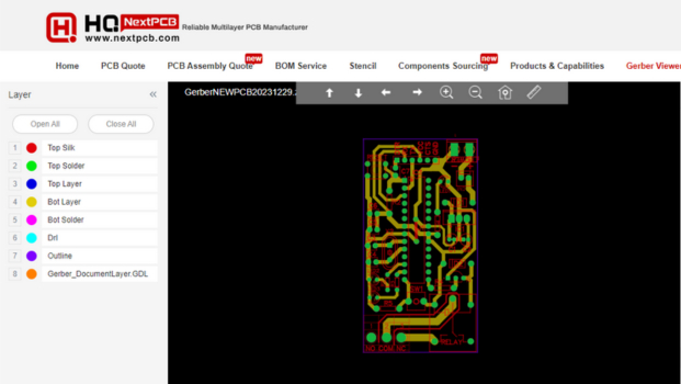
Key Features of NextPCB’s Layer-by-Layer Exploration:
Comprehensive Layer Analysis:
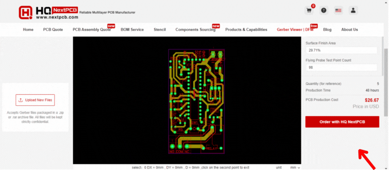
NextPCB’s HQDFM Free Online Gerber Viewer and DFM Analysis Tool redefine layer-by-layer navigation with its interactive layer-switching feature. Allowing designers to inspect individual layers such as copper, solder mask, and silkscreen. Designers can seamlessly toggle between different layers, exploring the intricate details of each without any hassle. This dynamic functionality provides a comprehensive view of the entire PCB design.
Zoom and Pan Capabilities:
Precision demands a closer look, and NextPCB delivers with its advanced zoom and pan capabilities. Designers can zoom in to scrutinize specific sections of a layer and pan across the design effortlessly, ensuring that no detail goes unnoticed. This level of control empowers designers to catch potential issues at a microscopic level.
Visibility Control:
Navigating complex PCB designs becomes more manageable with HQDFM’s visibility control. Designers can choose to display or hide specific layers, allowing for a focused examination of individual elements. This feature streamlines the analysis process, making it easier to identify and address potential manufacturing issues.
Cross-Sectional Analysis:
The layer-by-layer navigation extends beyond the two-dimensional view, offering cross-sectional analysis. Designers can delve into the depth of the PCB, examining the intricate layers that constitute the design. This three-dimensional perspective provides a holistic understanding of the design’s structural integrity.
Real-Time Updates:
As designers navigate through different layers, HQDFM provides real-time updates, ensuring that the displayed information is always current. This real-time feedback enables designers to make informed decisions on the fly, enhancing the efficiency of the design review process.
Layer-Specific DFM Analysis:
HQDFM’s layer-by-layer navigation is seamlessly integrated with DFM analysis. Designers can analyze each layer individually, focusing on specific manufacturing considerations. This integration enhances the tool’s ability to provide targeted feedback, allowing designers to address issues at a granular level.
Check PCB Manufacturing Data in the Smart Way
HQDFM offers designers a smart way to check PCB manufacturing data, providing a hassle-free and cost-effective Free Online Gerber Viewer. Visualize your PCB layouts with precision and clarity without the burden of cost constraints. The tool supports various Gerber file formats, ensuring flexibility and ease of use for designers at every level.
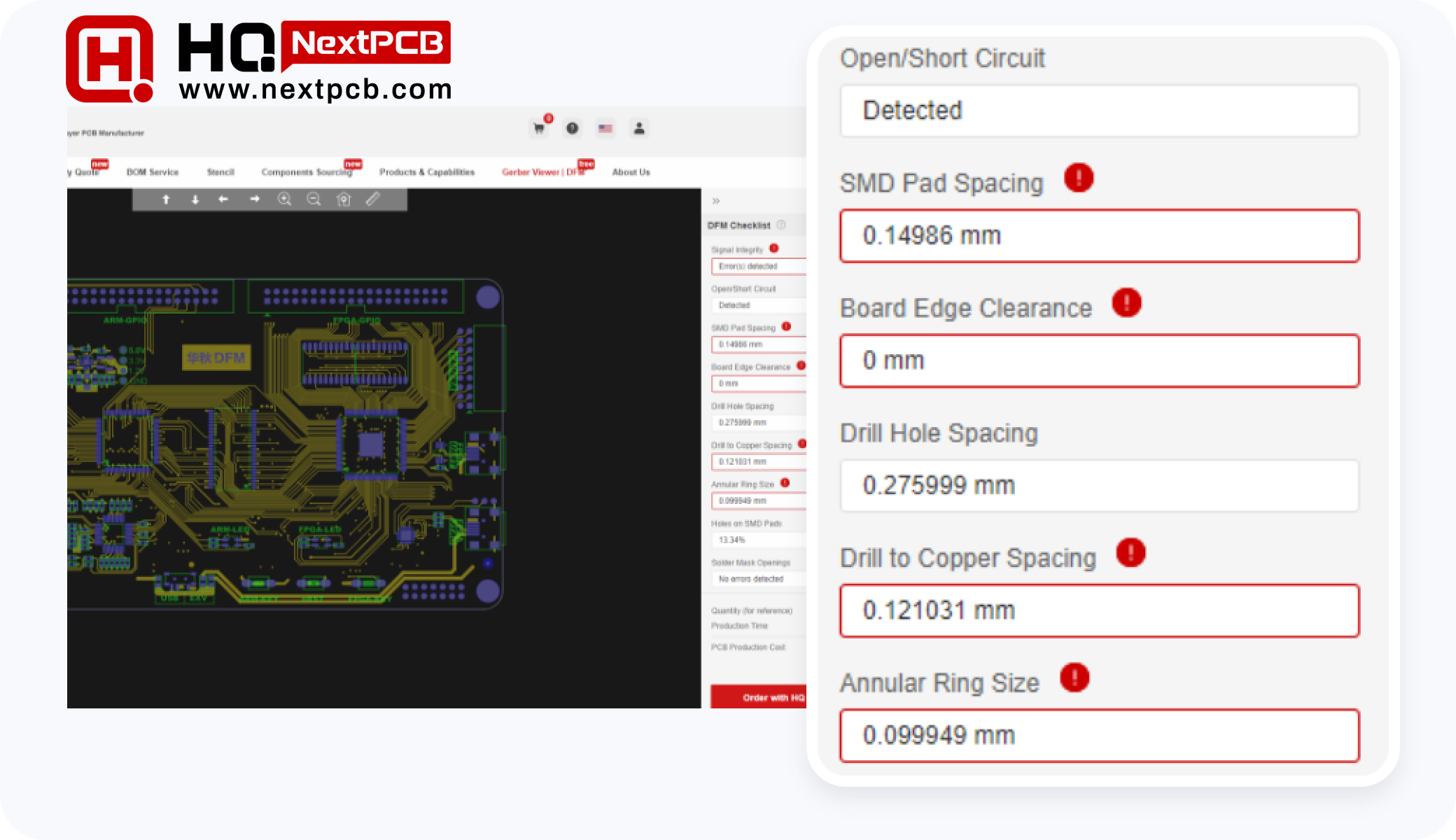
Detailed Error Reports and Suggestions
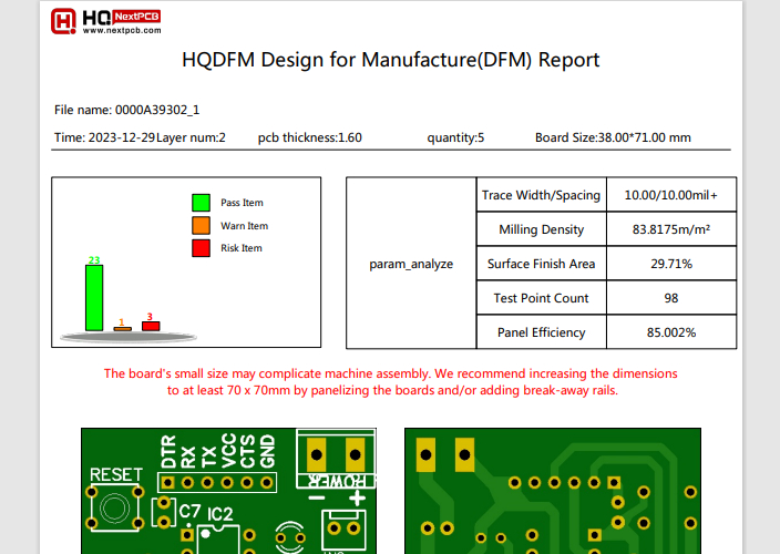
One of the standout features of NextPCB’s HQDFM Gerber Viewer is it generates detailed error reports, offering detailed insights into potential issues within the design. The tool scans Gerber files for potential issues such as spacing violations, trace width deviations, solder mask errors, and other critical parameters. It also provides actionable suggestions for resolution. This level of detail enables designers to address issues promptly. This also proactive approach ensures that designers catch issues early in the design phase, minimizing the risk of costly revisions and streamlining the entire design-to-manufacture journey.
Fast-Track Ordering with HQ NextPCB
HQDFM isn’t just a standalone tool; it’s part of the larger NextPCB ecosystem. The integration with NextPCB’s manufacturing services is where HQDFM truly shines. Fast-track your journey from design validation to production seamlessly. Once you’ve identified and addressed potential issues using the DFM analysis tool, the transition to placing orders for PCB fabrication and assembly is a breeze. HQDFM ensures that your designs not only meet but exceed manufacturing standards, allowing you to fast-track your orders with confidence.
Free PCB Assembly Service
The standout feature of NextPCB.com’s Free PCB Assembly service is the elimination of assembly costs. This means that designers can access professional PCB assembly services without the financial burden typically associated with prototyping. Quality is not compromised in this cost-free endeavor, as the service includes the use of high-grade components, ensuring prototypes meet the same standards as those produced through traditional assembly methods.
One of the most notable aspects of this service is the absence of minimum order quantity (MOQ) requirements. Whether a designer needs a single prototype or a small batch, they can leverage the Free PCB Assembly service without any restrictions, providing flexibility for projects of various scales.
Comprehensive testing services are an integral part of the Free PCB Assembly service, ensuring the functionality and reliability of the assembled prototypes. This commitment to quality control offers an added layer of assurance for designers, instilling confidence in the prototyping process.