
Why Designers Need to Pay Extra Attention to PCB Copper Thickness
Why Designers Need to Pay Extra Attention to PCB Copper Thickness
In PCB (Printed Circuit Board) design, copper thickness is often treated as a “standard parameter” and overlooked, with more attention given to component layout, routing topology, and impedance matching. However, copper thickness plays a crucial role as the core medium for PCB conductivity, heat dissipation, and mechanical structure. Whether its selection is appropriate directly determines the performance limits, reliability, and manufacturing costs of the board, and can even become the “hidden trigger” for mass product failures. For designers striving for optimal performance and stable mass production, paying extra attention to copper thickness is not redundant but rather a key factor that ensures design feasibility and long-term product stability.
Core Definition and Industry Standards for Copper Thickness
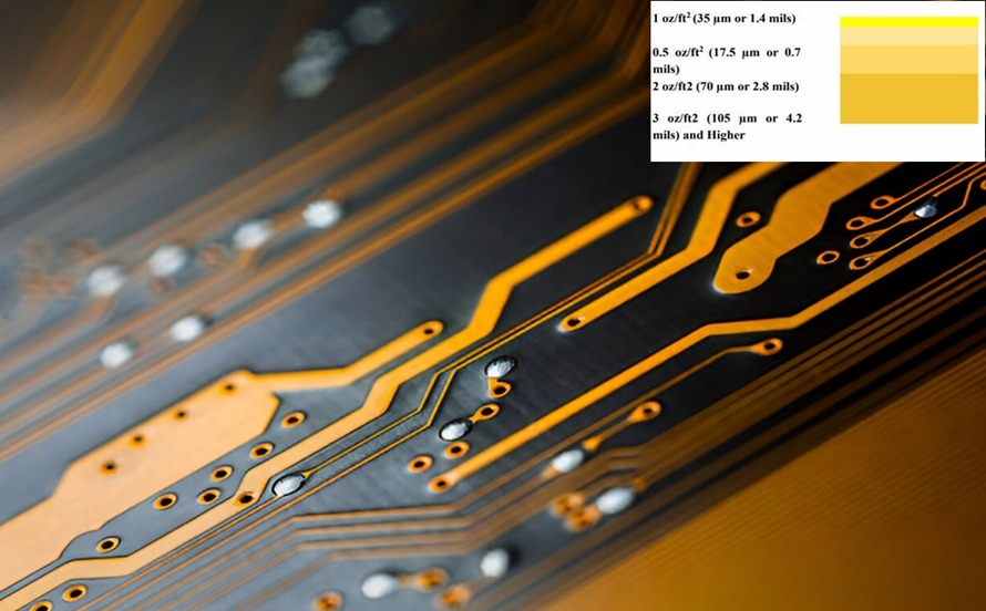
PCB copper thickness is typically measured in “ounces (oz),” which refers to the weight of copper foil per square foot. This weight is then converted to actual thickness using copper’s density (8.96 g/cm³). A 1 oz copper foil corresponds to a thickness of approximately 35 μm (exact value: 34.79 μm), which is a fundamental conversion standard in the electronics industry. Common specifications include 0.5 oz (17.5 μm), 1 oz (35 μm), and 2 oz (70 μm), with thick copper options ranging from 3 oz (105 μm) to 10 oz (350 μm) or even thicker.
It’s important to note that copper thickness must comply with IPC standards: IPC-4562 specifies that 1 oz copper foil should have an actual thickness between 32.2 μm and 37.8 μm. Deviations beyond this range directly affect current carrying capacity. For example, if the thickness is below 32 μm, the current carrying capacity drops by 10%. IPC-2152 provides the core basis for calculating copper layer current capacity, which needs to consider factors such as environmental temperature, trace width, and internal/external layer layout. Additionally, finished copper thickness and base copper thickness are not the same. The outer copper thickness is typically the sum of the base copper and electroplated copper. For instance, a 1 oz finished copper thickness can be achieved by plating 0.5 oz base copper. Designers should clearly indicate the finished copper thickness and tolerance range in the Gerber files.
Key Reasons for Extra Attention to Copper Thickness
(a) Determines Current Carrying Capacity
Copper is the primary conductive material in PCBs, and its thickness directly affects the cross-sectional area of traces, which in turn impacts resistance and the maximum current capacity. According to Ohm’s Law, with fixed trace width and length, thicker copper layers result in lower resistance and higher current capacity, while also reducing the heat generated according to Joule’s Law (Q=I²Rt). Industry data shows that ignoring the width’s influence, each increase of 1 oz in copper thickness can increase current carrying capacity by 50%–80%. The current carrying capacity of 1 oz copper foil can differ by more than 2 times compared to 3 oz copper foil.
Different copper thicknesses have clear differences in current carrying capacity (at 25°C and under long-term working conditions): A 0.5 oz copper foil of 1 mm width can carry 0.5–0.8 A, suitable for low-current scenarios like TWS headphones; 1 oz copper foil can carry 1.0–1.5 A, meeting the needs of standard signal traces like those on smartphone motherboards; 2 oz copper foil can carry 1.8–2.5 A, suitable for medium-current scenarios like automotive BMS; 3 oz copper foil can carry 2.8–3.5 A, used in high-power applications like industrial inverters.
If designers ignore the matching between copper thickness and current requirements, using too thin copper foil for high currents will cause the copper foil temperature to rise sharply, leading to copper foil melting, pad detachment, substrate carbonization, or even fire. On the other hand, blindly using excessively thick copper foil increases material and processing costs, which may not be cost-effective.
(b) Affects Heat Dissipation Efficiency
As electronic products continue to evolve toward higher power and miniaturization, PCB heat dissipation performance has become a key factor affecting product reliability. Copper layers serve as the core medium for heat dissipation in PCBs. Copper’s thermal conductivity is around 401 W/(m·K), over 800 times that of FR-4 substrates (0.3–0.5 W/(m·K)), meaning copper thickness directly affects heat transfer efficiency.
Thicker copper layers provide larger heat conduction areas, distribute heat more evenly, and quickly transfer heat generated by components to heat sinks or the entire PCB, reducing local hotspot temperatures. For example, an automotive MCU (with 3W power consumption) using 1 oz copper foil can reach a surface temperature of 85°C. By switching to 2 oz copper foil, the temperature drops to 72°C, fully meeting the automotive electronic operating temperature range of -40 to 125°C. On the contrary, thin copper foil causes heat buildup, which accelerates component aging and may result in solder joint failure, signal drift, and particularly affect high-temperature components such as power chips and LED drivers.
Moreover, designers can enhance overall heat dissipation efficiency by adding copper in blank areas of the PCB and using appropriate copper thickness, creating additional heat spreading paths. This is an essential aspect of optimizing both copper thickness and thermal design.
(c) Ensures Signal Integrity
For high-frequency (>1 GHz) and high-speed digital signals (such as DDR5 and 5G RF), copper thickness has a significant impact on signal integrity, particularly regarding skin effect and impedance control. Skin effect refers to the phenomenon where high-frequency currents tend to concentrate on the surface of conductors. At a frequency of 1 GHz, the current’s skin depth is about 6.6 μm. In such cases, overly thick copper foil can increase surface roughness, causing signal attenuation. For instance, 1 oz copper foil increases signal attenuation by 0.2 dB/cm compared to 0.5 oz copper foil at 10 GHz.
The precise control of characteristic impedance is crucial for high-speed signal transmission. Impedance depends on trace width, dielectric thickness, and copper thickness. Overly thick copper layers can cause traces to have a tapered cross-section (etching side-etching effect), deviating from the designed rectangular cross-section and affecting impedance accuracy. Uneven copper thickness can lead to impedance differences in different regions, resulting in signal reflection and increased crosstalk. Therefore, high-frequency, high-speed PCBs typically prioritize the use of 0.5 oz to 1 oz thin copper foil, balancing etching accuracy and impedance stability, while low-speed signals (<100 MHz) are less sensitive to copper thickness and can focus more on current requirements.
(d) Enhances Mechanical Stability
PCBs are not only electrical carriers but also an essential part of the product’s mechanical structure. Copper thickness directly influences its mechanical strength and soldering reliability. Proper copper thickness improves the PCB’s resistance to bending, reducing issues such as trace cracking and pad detachment caused by thermal stress during transportation or use. Moreover, thicker copper foil enhances pad strength, reducing mechanical stress caused by connector insertion, heavy component load, and minimizing cold solder or false solder issues.
Different applications require varying levels of mechanical strength: Automotive, industrial control, and other products subject to harsh environments require more stringent copper thickness, typically using 2 oz or thicker copper. Flexible PCBs, such as those in foldable smartphones, require flexibility, often using 0.3–2 oz rolled copper foil (with low surface roughness and good ductility), rather than non-standard electroplated copper foil. If the copper layer is too thin, the PCB’s mechanical strength will be insufficient, making it prone to scratches or tears during manufacturing or assembly, significantly reducing product yield.
(e) Adapts to Manufacturing Processes
Copper thickness directly affects PCB processing difficulty, impacting mass production yield and manufacturing costs. Thin copper foil (≤0.5 oz) is easier to etch into fine traces and is suitable for high-density interconnect (HDI) applications, but it is prone to wrinkling or shifting during lamination, making it difficult to precisely control trace width and spacing during etching, which can lead to over-etching or side-etching issues. On the other hand, ultra-thick copper foil (>2 oz) requires longer etching time and may result in the “mushroom effect” (plating forming mushroom heads), decreasing trace precision. Additionally, thick copper foil is harder and can cause resin underfill issues during lamination, leading to interlayer voids and accelerating drill bit wear during hole drilling, thus increasing processing costs.
Moreover, copper is a major component of PCB material costs. Every increase of 1 oz in copper thickness significantly raises both material and processing costs. Designers who fail to choose the right copper thickness based on the manufacturer’s process capabilities may face challenges in mass production or low yield rates. For example, an engineer chose 1 oz copper foil for an automotive BMS, which led to a 95°C copper foil temperature (exceeding the safety limit of 85°C) under 2A current. By switching to 2 oz copper foil, the issue was resolved, ensuring performance and avoiding mass rework costs.
Core Principles and Practical Recommendations for Copper Thickness Selection
Choosing the right copper thickness is not about “the thicker, the better”; instead, it requires balancing electrical performance, heat dissipation needs, mechanical strength, manufacturing processes, and costs. The core principle is “matching the requirements”. Here are some practical recommendations:
Accurate Current Capacity Calculation: Consider the maximum operating current, ambient temperature, and trace width. Refer to the IPC-2152 standard to calculate the minimum copper thickness, with a safety margin of 10% to 20%, to avoid insufficient current handling.
Match Signal Type: For high-frequency and high-speed scenarios, prioritize using 0.5 oz to 1 oz thin copper. For low-speed, high-current scenarios, choose copper thickness of 2 oz or more. For RF applications, rolled copper foil can be used to improve signal quality.
Consider Heat Dissipation Needs: Use thicker copper foil around high-power components (such as power chips) and combine copper-pouring designs to create efficient heat dissipation paths.
Adapt to Manufacturing Capabilities: Communicate thoroughly with EMS PCB manufacturers to understand their processing accuracy and tolerance ranges for different copper thicknesses. This ensures that the design stays within the manufacturing limits.
Clear Labeling of Requirements: Clearly specify the finished copper thickness (distinguishing between inner and outer layers) and tolerance range in the manufacturing drawings. Avoid ambiguity that could result in copper thickness deviations.
Conclusion
The copper thickness of a PCB may seem like a small design parameter, but it affects the entire lifecycle of a product — from design, manufacturing, to usage. It directly impacts performance, reliability, and cost. In today’s competitive electronics market, designers must not only focus on achieving core functionalities but also pay attention to “detail parameters” like copper thickness. Ignoring it may lead to mass product failure and uncontrolled costs, while focusing on it allows for balancing performance, yield, and cost efficiency.
For PCB designers, paying extra attention to copper thickness is, in essence, about establishing a “full-process design mindset”, integrating electrical, thermal, mechanical design, and manufacturing processes. Only in this way can we create PCBs that meet design specifications, adapt to mass production needs, and offer both stability and cost-effectiveness — giving our products a competitive edge in the market.