

555 Timer IC – Pinout, Specifications & Working Principle
Hello friends! Welcome back to ElectroDuino. This blog is base on the 555 Timer IC. Here we will discuss the Introduction to 555 Timer IC, IC pin diagram, operating modes, Features, 555 Timer IC Equivalent, and applications.
Introduction
555 Timer IC one of the most popular and most used ICs of all time. This IC was designed by Hans R in 1971. Camenzind. This IC can be used as a time delay, as an oscillator, and as a flip-flop element among other applications.
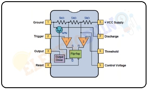
IC Pin Configuration
|
Pin Number |
Pin |
Pin Description |
|
1 |
Ground |
The ground reference voltage (zero volts). |
|
2 |
Trigger |
Pin-2 is a trigger pin that is Responsible for the transition of the flip-flop from set to reset. The 555 timer OUT Pin goes high and a timing interval starts when the trig pin input voltage falls below ½ of CONTROL voltage. So simply we can say that The output of the timer depends on the amplitude of the external trigger pulse that is applied to the trigger pin |
|
3 |
Output |
Pin-3 is an output pin, which is normally connected to a load. There are two ways in which a load can be connected to the output terminal. |
|
4 |
Reset |
pin-4 is the reset terminal, which is used to disable or reset the timer. When a negative pulse is applied to pin 4 then IC becomes reset or disable. Hence if this pin is not to be used for reset purposes, it should be connected to + VCC to avoid any possibility of false triggering. |
|
5 |
Control |
Pin-5 is the control voltage pin. It provides access to the internal voltage divider (2⁄3 VCC by default). This pin used to control the pulse width of the output waveform and also the levels of threshold and trigger. In most applications this pin is not used, this time it should be connected to ground through a 10 nF (0.01µF) capacitor to avoid any noise problem. |
|
6 |
Threshold |
Pin-6 is the threshold pin, This is the non-inverting input terminal of comparator 2, the timing (OUT high) interval ends when the voltage at this pin is greater than the voltage at the CONTROL pin. The set state of the flip-flop can depend on the amplitude of the threshold pin. |
|
7 |
Discharge |
Pin-7 is the discharge pin, it’s can be used to discharge a capacitor between intervals, in phase with output. |
|
8 |
Supply |
Pin-8 is the voltage supply pin, the applied voltage on this pin usually between + 5 V to + 18V with respect to ground (pin 1). |
Operating Modes of 555 Timer IC
555 timer operating modes are astable, bistable, and monostable.
Astable Mode :
In this mode the output pin produced rectangular pulses having a specific frequency. This astable mode circuit is implemented using two Resistor R1, R2, and one capacitor C. The output frequency depends on the value of R1, R2, and C.When the voltage is applied to the circuit, the capacitor continuously gets charged through two resistors and generates pulses continuously. In this circuit the control pin is not used, it is connected to ground through a 10 nF capacitor to avoid electrical noise. The frequency calculation is shown in the below figure.


Monostable Mode :
In this mode, the 555 Timer IC output pin generates only a single pulse. The 555 Timer IC output pulse ends when the voltage on the capacitor equals 2⁄3 of the supply voltage. This Pulse width can depend on the adjusting values of the resistor and capacitor. capacitor If an activating pulse is applied to the i/p of the circuit through a push-button, then the capacitor gets charged and the timer circuit extends a high pulse, then it remains high until the capacitor totally discharges.
The output pulse width of time t is given by
t = ln(3) . R . C
Where
t is in seconds (time),
R is in ohms (resistance),
C is in farads (capacitance),
ln(3) is the natural log of 3 constant

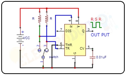
Bistable Mode :
In Bistable mode, the output pin produces 2-stable state signals which are LOW and HIGH. The output waveform is controlled by the trigger and reset inputs of the 555 timer IC. These pins are held “HIGH” using the two pull-up resistors, R1 and R2. When the switch is connected to set position than trigger input is “LOW” and as a result, the output set into “HIGH”. Similarly when the switch is connected to the set position then reset input is “LOW” and as a result, the output set into “LOW”.
Features of the 555 timer IC
| Parameter | Value |
| Supply voltage (VCC) | 4.5 to 15 V |
| Supply current (VCC = +5 V) | 3 to 6 mA |
| Supply current (VCC = +15 V) | 10 to 15 mA |
| Output current (maximum) | 200 mA |
| Maximum Power dissipation | 600 mW |
| Power consumption (minimum operating) | 30 mW@5V, 225 mW@15V |
| Operating temperature | 0 to 75 °C |
555 Timer IC Equivalent
NE555, LM555, NE556, LM556,
Applications
- Pulse generation
- Pulse Width Modulation
- Time Delay Generation
- Precision Timing
- Sequential Timing circuits


Pingback: PIR Sensor Burglar Alarm System Circuit using 555 Timer IC »